
Furthermore GTX 480 and GF100 were clearly not the products that NVIDIA first envisioned. We never saw a product using GF100 ship with all of its SMs enabled – the consumer space topped out at 15 of 16 SMs, and in the HPC space Tesla was only available with 14 of 16 SMs. Meanwhile GF100’s younger, punchier siblings put up quite a fight in the consumer space, and while they never were a threat to GF100, it ended up being quite the surprise for how close they came.
Ultimately the Fermi architecture at the heart of this generation is solid – NVIDIA had to make some tradeoffs to get a good gaming GPU and a good compute GPU in a single product, but it worked out. The same can’t be said for GF100, as its large size coupled with TSMC’s still-maturing 40nm process lead to an unwieldy combination that produced flakey yields and leaky transistors. Regardless of who’s ultimately to blame, GF100 was not the chip it was meant to be.
But time heals all wounds. With GF100 out the door NVIDIA has had a chance to examine their design, and TSMC the chance to work the last kinks out of their 40nm process. GF100 was the first Fermi chip, and it would not be the last. With a lesson in hand and a plan in mind, NVIDIA went back to the drawing board to fix and enhance GF100. The end result: GF110, the next iteration of Fermi. Hot out of the oven, it is launching first in the consumer space and is forming the backbone of the first card in NVIDIA’s next GeForce series: GeForce 500. Launching today is the first such card, the GF110-powered GeForce GTX 580.
| GTX 580 | GTX 480 | GTX 460 1GB | GTX 285 | |
| Stream Processors | 512 | 480 | 336 | 240 |
| Texture Address / Filtering | 64/64 | 60/60 | 56/56 | 80 / 80 |
| ROPs | 48 | 48 | 32 | 32 |
| Core Clock | 772MHz | 700MHz | 675MHz | 648MHz |
| Shader Clock | 1544MHz | 1401MHz | 1350MHz | 1476MHz |
| Memory Clock | 1002MHz (4008MHz data rate) GDDR5 | 924MHz (3696MHz data rate) GDDR5 | 900Mhz (3.6GHz data rate) GDDR5 | 1242MHz (2484MHz data rate) GDDR3 |
| Memory Bus Width | 384-bit | 384-bit | 256-bit | 512-bit |
| Frame Buffer | 1.5GB | 1.5GB | 1GB | 1GB |
| FP64 | 1/8 FP32 | 1/8 FP32 | 1/12 FP32 | 1/12 FP32 |
| Transistor Count | 3B | 3B | 1.95B | 1.4B |
| Manufacturing Process | TSMC 40nm | TSMC 40nm | TSMC 40nm | TSMC 55nm |
| Price Point | $499 | ~$420 | ~$190 | N/A |
But before we get too deep in to GF110, let’s start with today’s launch card, the GeForce GTX 580. GTX 580 is the first member of the GeForce 500 series, giving it the distinction of setting precedent for the rest of the family that NVIDIA claims will soon follow. Much like AMD last month, NVIDIA is on their second trip with the 40nm process, meaning they’ve had the chance to refine their techniques but not the opportunity to significantly overhaul their designs. As a result the 500 series is going to be very familiar to the 400 series – there really aren’t any surprises or miracle features to talk about. So in many senses, what we’re looking at today is a faster version of the GTX 480.
So what makes GTX 580 faster? We’ll start with the obvious: it’s a complete chip. All the L2 cache, all the ROPs, all the SMs, it’s all enabled. When it comes to gaming this is as fast as GF110 can be, and it’s only through NVIDIA’s artificial FP64 limitations that double-precision computing isn’t equally unrestricted. We have wondered for quite some time what a full GF100 chip would perform like – given that GTX 480 was short on texture units, shaders, and polymorph engines, but not ROPs – and now the answer is at hand. From all of this GTX 580 has 6.6% more shading, texturing, and geometric performance than the GTX 480 at the same clockspeeds. Meanwhile the ROP count and L2 cache remains unchanged; 48 ROPs are attached to 768KB L2 cache, which in turn are attached to 6 64bit memory controllers.
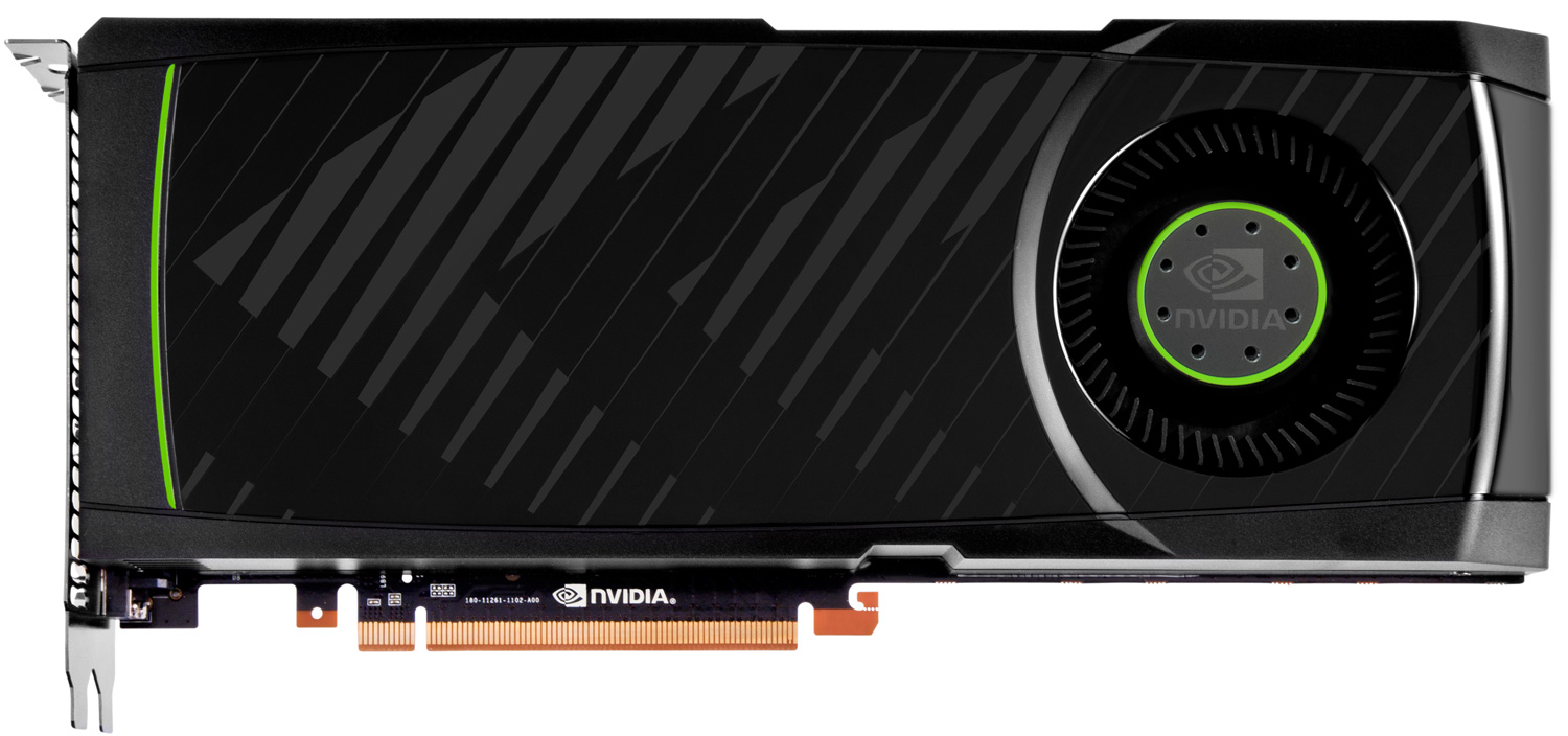
GeForce GTX 580
Last but certainly not least change coming from GTX 480 is in GF110 itself. NViDIA has ported over GF104’s faster FP16 (half-precision) texture filtering capabilities, giving GF110/GTX580 the ability to filter 4 FP16 pixels per clock, versus 2 on GF100/GTX480. The other change ties in well with the company’s heavy focus on tessellation, with a revised Z-culling/rejection engine that will do a better job of throwing out pixels early, giving GF110/GTX580 more time to spend on rendering the pixels that will actually be seen. This is harder to quantify (and impossible for us to test), but NVIDIA puts this at another 8% performance improvement.
Meanwhile NVIDIA hasn’t ignored GTX 480’s hot and loud history, and has spent some time working on things from that angle. We’ll dive in to NVIDIA’s specific changes later, but the end result is that through some optimization work they’ve managed to reduce their official TDP from 250W on the GTX 480 to 244W on the GTX 580, and in practice the difference is greater than that. NVIDIA’s cooling system of choice has also been updated, working in tandem with GTX 580’s lower power consumption to bring down temperatures and noises. The end result is a card that should be and is cooler and quieter while at the same being faster than GTX 480.

GF110
In any case, with GTX 580 taking the $500 spot and GF110 ultimately destined to replace GF100, GF100 based cards are going to be on their way out. NVIDIA doesn’t have an official timeline, but we can’t imagine they’ll continue producing GF100 GPUs any longer than necessary. As a result the GTX 480 and GTX 470 are priced to go, falling between the GTX 580 and the GTX 460 in NVIDIA’s lineup for now until they’re ultimately replaced with other 500 series parts. For the time being this puts the GTX 480 at around $400-$420, and the GTX 470 – still doing battle with the Radeon HD 6870 – is at $239-$259.
Meanwhile AMD does not have a direct competitor for the GTX 580 at the moment, so their closest competition is going to be multi-GPU configurations. In the single card space there’s the Radeon HD 5970, which is destined for replacement soon and as a result AMD is doing what they can to sell off Cypress GPUs by the end of the year. The last reference 5970 you can find on Newegg is a Sapphire card, which is quite blatantly priced against the GTX 580 at $499 with a $30 rebate. Given that it’s the last 5970, we’d be surprised if it was in stock for much longer than the initial GTX 580 shipments.
For cards you do stand a good chance of getting, a pair of 6870s will set you back between $480 and $500, making it a straightforward competitor to the GTX 580 in terms of price. A pair of cards isn’t the best competitor, but CrossFire support is widely available on motherboards so it’s a practical solution at that price.
| Fall 2010 Video Card MSRPs | ||
| NVIDIA | Price | AMD |
| GeForce GTX 580 | $500 | Radeon HD 5970 |
| $420 | ||
| | $300 | Radeon HD 5870 |
| $240 | Radeon HD 6870 | |
| $180 | Radeon HD 6850 | |
No comments:
Post a Comment
If you have any Doubt..kindly let me know