
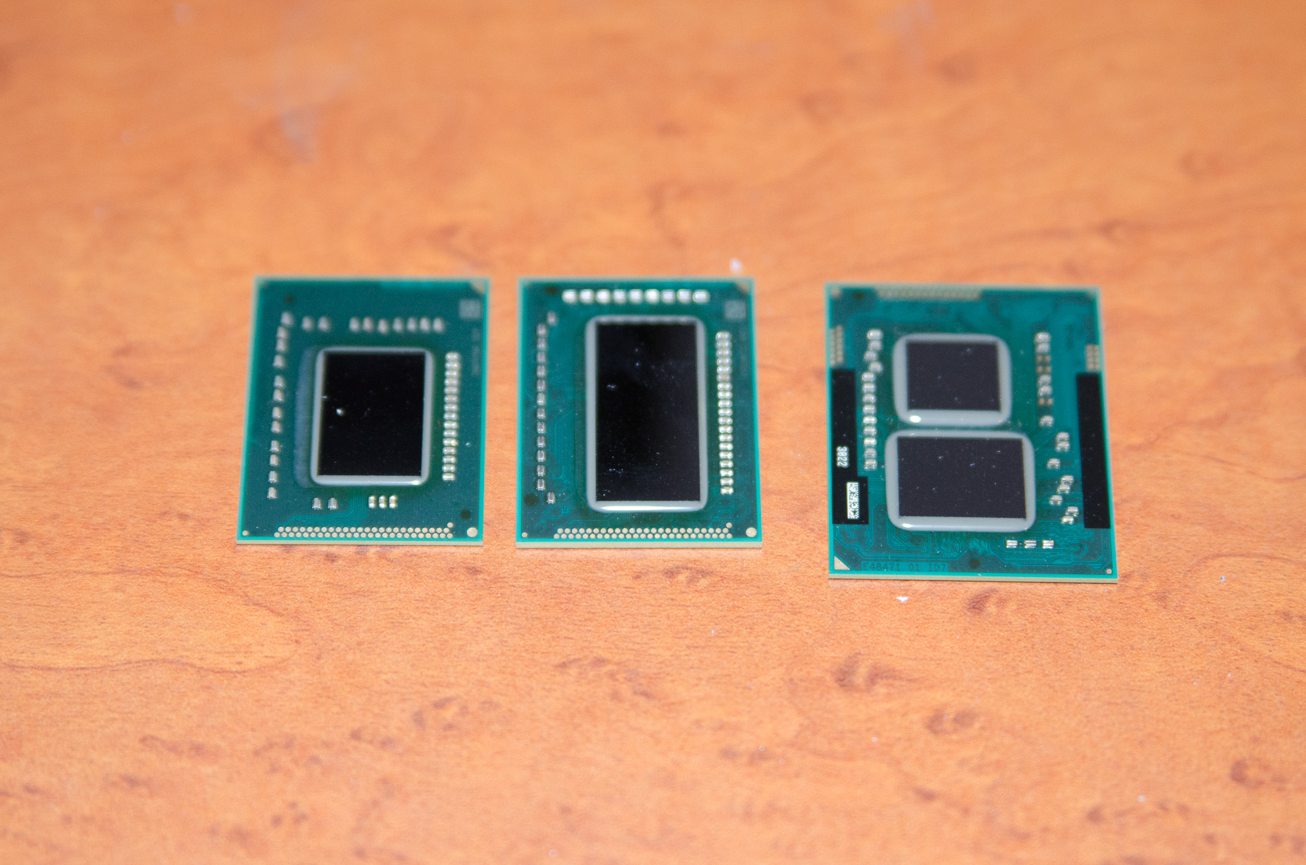
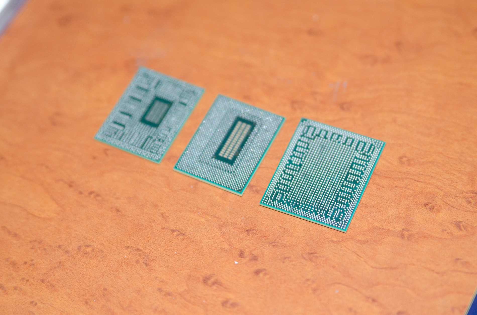
Aside from a stack of Reese’s Peanut Butter Cups, I snagged something else of interest at my Intel meeting at CES 2011: a shot of some exposed Sandy Bridge processor die. As a recap SNB is available in three different physical die versions today: quad-core, dual-core with GT1 graphics and dual-core with GT2 graphics. The die sizes and transistor counts are below:
| CPU Specification Comparison | ||||||||
| CPU | Manufacturing Process | Cores | Transistor Count | Die Size | ||||
| AMD Thuban 6C | 45nm | 6 | 904M | 346mm2 | ||||
| AMD Deneb 4C | 45nm | 4 | 758M | 258mm2 | ||||
| Intel Gulftown 6C | 32nm | 6 | 1.17B | 240mm2 | ||||
| Intel Nehalem/Bloomfield 4C | 45nm | 4 | 731M | 263mm2 | ||||
| Intel Sandy Bridge 4C | 32nm | 4 | 995M | 216mm2 | ||||
| Intel Lynnfield 4C | 45nm | 4 | 774M | 296mm2 | ||||
| Intel Clarkdale 2C | 32nm | 2 | 384M | 81mm2 | ||||
| Intel Sandy Bridge 2C (GT1) | 32nm | 2 | 504M | 131mm2 | ||||
| Intel Sandy Bridge 2C (GT2) | 32nm | 2 | 624M | 149mm2 | ||||
No comments:
Post a Comment
If you have any Doubt..kindly let me know