Saturday, October 2, 2010

Zacate and Ontario are due out in a quarter, and both promise to bring competition to an area where we haven’t seen much from AMD.

Llano is slated for release near the end of Q2 next year. While it won’t be a big step forward in CPU performance, we should see a huge increase in integrated graphics performance.

Sampling in Q4 of this year and shipping sometime next year is AMD’s next-generation microarchitecture: Bulldozer.

Within the course of twelve months we will see AMD introduce three drastically different microprocessors into the market’s eager hands. We’ve been dying for more competition and AMD is planning on giving us just that. But that's the future, what about the present?

Processor Clock Speed L2 Cache L3 Cache TDP Price
AMD Phenom II X6 1090T BE 3.2GHz 3MB 6MB 125W $295
AMD Phenom II X6 1075T 3.0GHz 3MB 6MB 125W $245
AMD Phenom II X6 1055T 2.8GHz 3MB 6MB 125W $199
AMD Phenom II X4 970 BE 3.5GHz 2MB 6MB 125W $185
AMD Phenom II X4 965 BE 3.4GHz 2MB 6MB 125W $165
AMD Phenom II X4 955 BE 3.2GHz 2MB 6MB 125W $145
AMD Phenom II X2 560 BE 3.3GHz 1MB 6MB 80W $105
AMD Phenom II X2 555 BE 3.2GHz 1MB 6MB 80W $93
AMD Athlon II X4 645 3.1GHz 2MB 0MB 95W $122
AMD Athlon II X4 640 3.0GHz 2MB 0MB 95W $100
AMD Athlon II X3 450 3.2GHz 1.5MB 0MB 95W $87
AMD Athlon II X3 445 3.1GHz 1.5MB 0MB 95W $76
AMD Athlon II X2 265 3.3GHz 2MB 0MB 65W $76
AMD Athlon II X2 260 3.2GHz 2MB 0MB 65W $69
AMD Athlon II X2 255 3.1GHz 2MB 0MB 65W $66

Today AMD announced speed bumps to nearly every processor in its desktop lineup. Everything from the dual-core Athlon II to the six-core Phenom II gets a new family member today. And they’re all very attractively priced.

A Third Phenom II X6

We’ll start at the high end. The Phenom II X6 line expands to include a 3.0GHz 1075T. Smack in the middle of the other X6s, the 1075T will set you back $245 and can turbo up to 3.5GHz if three or fewer cores are in use. You get a 6MB L3 and a 3MB L2 (512KB per core).

The Phenom II X6 1075T has no competitively priced answer from Intel. The Core i7 860 is priced at $284, while the Core i5 760 will set you back $205. The default clock speed of the 1075T should bring it close to the Core i5 760 in many tasks, while anything threaded will for sure favor the 1075T. Remember the quad-core i5s lack Hyper Threading so this is a 6 core/6 thread chip matched up against a 4/4. Intel’s cores get better performance per clock, but not that much better. Single threaded performance and power consumption are both advantages of the Core i5, but the rest will easily fall in AMD’s favor.

A 3.5GHz Quad-Core

It’s not all about more cores from AMD. The new Phenom II X4 970 Black Edition pushes quad-core clock speed to 3.5GHz. The 970 ships with all cache enabled, so that's 6MB L3 and 2MB total L2.

This is still a Deneb so you get no core turbo support, but you do get a great value. At $185 the Phenom II X4 970 only has to compete with the Core i5 750 or a bunch of dual-core Clarkdale CPUs. Without Hyper Threading, the matchup can be close. AMD and Intel trade blows here, with Intel typically ending up on top. Single threaded performance is close as AMD has a huge clock speed advantage. AMD gets the nod for slightly lower price and better upgrade path as you’ll can stick a Phenom II X6 in the same Socket-AM3 motherboard. Bulldozer is out of the question however, AM3+ chips aren’t backwards compatible with AM3 motherboards (although the opposite is true, you will be able to use your 970 in an AM3+ motherboard).

Value Quad-Core at 3.1GHz

Next on the list is a value quad-core offering, the Athlon II X4 645 is a speed bump of one of the most attractive quad-core CPUs we’ve ever reviewed. The Athlon II X4 does away with an L3 cache in order to keep costs down while keeping the same 512KB private L2 per core (2MB total). The 645 runs at 3.1GHz and will set you back $122.

Intel has no competition for this processor. The Core i3 540 is priced similarly but you only get two cores. Intel is faster in lightly threaded apps and games, but AMD is faster everywhere else. If you’re a multitasker my vote goes for the Athlon II X4 645. Intel does offer lower power consumption and on-chip graphics if you’re looking to build a HTPC.

High-End Dual-Core

AMD’s Phenom II X2 560 gives you two cores running at 3.3GHz and a full 6MB L3 cache. You only have to pay $105 to play.

In a stock fight, the 560 will easily lose to Intel’s Core i3 530. Both chips have two cores and the larger L3 cache doesn’t do much for AMD given Intel’s IPC advantage. The 560 however might come from a die harvested part. It may just be a Phenom II X4 but with two cores disabled. Assuming you get a good chip and have a motherboard with core-unlocking support, you might just find yourself with Phenom II X4 “960” and save $50. Proceed at your own risk. We could unlock three of the four cores on our chip but the system wasn’t stable enough to enter Windows with the extra unlocked core.

The Athlon II X3 450: A Pentium G6950 Killer

While AMD no longer lists a triple-core Phenom II on its price list, the Athlon II X3 is still alive and well. The new 450 gives you three cores at 3.2GHz for $87. This is a harvested part taken from quad-core chips, as a result you get no L3 cache and 1.5MB of total L2 on chip (512KB per core x 3). The closest competitor from Intel is the Pentium G6950.

AMD has the clock and core advantage, although Intel has a single threaded performance advantage. AMD wins across the board virtually regardless of application. The Athlon II X3 450 gives you more bang for your buck than the Pentium G6950.

Affordable Dual-Core

Last, but not least, we have the new Athlon II X2 265. Running at 3.3GHz and priced at only $76 you have to look at Intel’s previous-generation Penryn based processors to find a suitable competitor for this chip. There's no L3 cache but the L2 gets a bump to 2MB total (1MB per core).

Personally I’m not terribly interested in the 265. For an extra $11 you get an additional core and only lose 100MHz, a tradeoff that I believe is more than worth it.

The Test

To keep the review length manageable we're presenting a subset of our results here. For all benchmark results and even more comparisons be sure to use our performance comparison tool: Bench.

We've moved all of our AMD CPU testing to the 890GX platform. While nearly all numbers are comparable you may occasionally see some scaling that doesn't quite add up compared to lower clocked versions of the same chips running on a previous motherboard.

Motherboard: ASUS P7H57DV- EVO (Intel H57)
Intel DP55KG (Intel P55)
Intel DX58SO (Intel X58)
Intel DX48BT2 (Intel X48)
ASUS M4A89GTD Pro/USB3 (AMD 890GX)
Chipset Drivers: Intel 9.1.1.1015 (Intel)
AMD Catalyst 8.12
Hard Disk: Intel X25-M SSD (80GB)
Memory: Corsair DDR3-1333 4 x 1GB (7-7-7-20)
Corsair DDR3-1333 2 x 2GB (7-7-7-20)
Video Card: eVGA GeForce GTX 280 (Vista 64)
ATI Radeon HD 5870 (Windows 7)
Video Drivers: ATI Catalyst 9.12 (Windows 7)
NVIDIA ForceWare 180.43 (Vista64)
NVIDIA ForceWare 178.24 (Vista32)
Desktop Resolution: 1920 x 1200
OS: Windows Vista Ultimate 32-bit (for SYSMark)
Windows Vista Ultimate 64-bit
Windows 7 x64

Read more...
HP Mini 5102: This Netbook Means Business


Netbooks are an interesting category of mobile device; some people love them and others loathe them. We definitely wouldn’t want to be stuck with a netbook as our primary computing device, and probably not even our primary laptop. HP actually understands this quite well with the 5102 and markets it as a companion device for business users, with some interesting features to back up that claim. This is a “mini executive” laptop that would pair up very nicely with a ProBook or EliteBook if you’re part of the HP ecosystem.

We should note that the 5102 is actually an older model and it has since been replaced by the 5103, which uses the same basic chassis and design but switches to DDR3 enabled Atom CPUs. So why are we reviewing this older laptop? For one, it’s still on sale, and prices have dropped quite a bit since its introduction making it a more interesting option. The other reason is pretty typical: HP offered to send us a unit for review, and we figured, “why not?” We know what to expect from Atom N450 in terms of performance, but having looked at the ProBook and EliteBook we were interested to see HP’s “Business Mini” in person. Most of what we have to say about the 5102 applies to the 5103 as well, except we’d expect better battery life and slightly better performance from the newer model—though the N550 CPU might cut battery life in pursuit of performance. So with that disclaimer out of the way, let’s see what the Mini 5102 has to offer.

The basic feature set for the 5102 is the same as what you’ll find with many Atom netbooks, but HP has some extra features in the way of software to make it more useful. One set of software is HP QuickSync, which keeps your Mini synced up with your desktop’s email, documents, images, etc. This makes it very easy to pick up the Mini and head out for meetings, without having to worry about manually transferring your data. HP also includes Corel Home Office, which allows users to view and edit MS Office files without the need to spend a bunch of money on a fully licensed version of MS Office. The remaining features aren’t particularly noteworthy, but let’s give a rundown of the specifications of the Mini 5102.

HP Mini 5102 Specifications
Processor Intel Atom N450
(1.66GHz + SMT, 45nm, 512KB L2, 533FSB, 5.5W)
Chipset Intel NM10
Memory 1x1024MB DDR2-800 @ DDR2-667 5-5-5-15 Timings
Graphics Integrated Intel GMA 3150
Display 10.1" LED Matte 16:9 WSVGA (1024x600)
(LG Philips LP101WSA-TLB2)
Hard Drive 2.5" 160GB 7200RPM 8MB
(Western Digital WD1600BEKT-60V5T1)
Networking Marvel Yukon 88E8059 PCIe Gigabit Ethernet
Broadcom BCM43224 802.11a/b/g/n WiFi
Bluetooth 2.1 (Optional)
Audio IDT 92HD75B2X5 2-Channel HD Audio
(2.0 Speakers with headphone/microphone jacks)
Battery 4-Cell, 14.8V, 1900mAh, 29Wh
6-Cell, 11.25V, 5700mAh, 66Wh
Front Side None (Speaker Grille)
Left Side 2 x USB 2.0
Heat Exhaust
VGA
AC Power Connection
Right Side SD/MMC reader
Microphone/Headphone Jacks
Gigabit Ethernet
1 x USB 2.0
Kensington Lock
Back Side None
Operating System Windows 7 Starter
Dimensions 10.3" x 7.09" x 0.91" (WxDxH)
Weight 2.64 lbs (with 6-cell battery)
Extras 2.0MP Webcam
82-key keyboard
Broadcom Crystal HD (Optional)
Warranty 1-year standard warranty
Price Online starting at $388

Besides the regular items, the interesting additions include a matte LCD panel, 7200RPM hard drive, and—shock and awe!—a Gigabit Ethernet controller. The latter is particularly useful if you plan on using the QuickSync feature with larger files, though the estimated 14+ hours to do the initial sync with my desktop (and around 30GB of data) shows that QuickSync isn’t necessarily the fastest way to do things. The wireless network controller is also a higher end option than what most netbooks get, with 802.11a/b/g/n support (11a is used in businesses on occasion, though I’ve yet to see anyone using it at home).

Depending on where you pick up your Mini, you can custom configure the system. HP’s site has the Mini 5103, which is the same only it offers newer CPUs—including the new dual-core N550—and DDR3 memory. HP offers a Broadcom Crystal HD decoder upgrade for $45, and I’ve been wanting to test one of those for a while. I didn’t get one with the 5102, but Anand sent me his BCM70012 mini-PCIe card and I managed to install it (see page three for details). The 5103 starts out at $400 from HP, or the configurable options start at $450 (with the current 12% off coupon). The Mini 5102 can be purchased online from Newegg and others for around $400 as well. What that means is you’re paying about $100 extra for the build quality, software, and any other extras.

Skipping back to the 5103, the configurator allows quite a few potentially interesting upgrades. There’s the aforementioned Crystal HD card, or you can get Mobile Broadband. LCD alternatives are also present: besides the standard WSVGA model, you can get a touchscreen WSVGA or go for a 1366x768 panel. The problem is that all of the interesting upgrades add to the price of an already expensive netbook. If you want 2GB RAM, 128GB SSD, the 768p LCD, Crystal HD, and the 6-cell battery, you can get the price up to $1000. For a netbook! Drop the SSD and you’re still approaching $700, though, which is frankly obscene for anything with an Atom CPU beating in the chassis.

Our test system is the basic $400 model available at MWave and other vendors, but HP shipped us the 6-cell battery for testing as well, and we added our own Crystal HD card. Those two upgrades bring the price to around $500 if you go that route, but let’s see what the HP 5102 can deliver before we decide if the upgrades are worth having.


Read more...
GTC 2010 Day 1: NVIDIA Announces Future GPU Families for 2011 And 2013


in San Jose, California covering NVIDIA’s annual GPU Technology Conference. If Intel has IDF and Apple has the World Wide Developers Conference, then GTC is NVIDIA’s annual powwow to rally their developers and discuss their forthcoming plans. The comparison to WWDC is particularly apt, as GTC is a professional conference focused on development and business use of the compute capabilities of NVIDIA’s GPUs (e.g. the Tesla market).

NVIDIA has been pushing GPUs as computing devices for a few years now, as they see it as the next avenue of significant growth for the company. GTC is fairly young – the show emerged from NVISION and its first official year was just last year – but it’s clear that NVIDIA’s GPU compute efforts are gaining steam. The number of talks and the number of vendors at GTC is up compared to last year, and according to NVIDIA’s numbers, so is the number of registered developers.

We’ll be here for the next two days meeting with NVIDIA and other companies and checking out the show floor. Much of this trip is to get a better grasp on just where things are for NVIDIA still-fledging GPU compute efforts, especially on the consumer front where GPU compute usage has been much flatter than we were hoping for at this time last year with the announcement/release of NVIDIA and AMD’s next-generation GPUs, and the ancillary launch of APIs such as DirectCompute and OpenCL, which are intended to allow developers to write an application against these common APIs rather than targeting CUDA or Brook+/Stream. If nothing else, we’re hoping to see where our own efforts in covering GPU computing need to lie – we want to add more compute tests to our GPU benchmarks, but is the market to the point yet where there’s going to be significant GPU compute usage in consumer applications? This is what we’ll be finding out over the next two days.

Jen-Hsun Huang Announces NVIDIA’s Next Two GPUs

While we’re only going to be on the show floor Wednesday and Thursday, GTC unofficially kicked off Monday, and the first official day of the show was Tuesday. Tuesday started off with a 2 hour keynote speech by NVIDIA’s CEO Jen-Hsun Huang, which keeping with the theme of GTC focused on the use of NVIDIA GPUs in business environments.

Not unlike GTC 2009, NVIDIA is also using the show as a chance to announce their next-generation GPUs. GTC 2009 saw the announcement of the Fermi family, with NVIDIA first releasing the details of the GPU’s compute capabilities there, before moving on to focusing on gaming at CES 2010. This year NVIDIA announced the next two GPU families the company is working on, albeit not in as much detail as we got about Fermi in 2009.


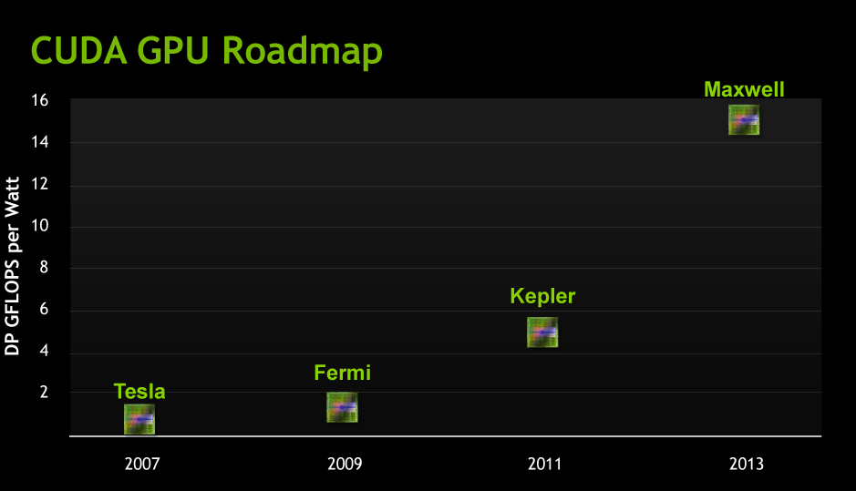
The progression of NVIDIA's GPUs from a Tesla/Compute Standpoint

The first GPU is called Kepler (as in Johannes Kepler the mathematician), which will be released in the 2nd half of 2011. At this point the GPU is still a good year out, which is why NVIDIA is not talking about its details just yet. For now they’re merely talking about performance in an abstract manner, in this case Kepler should offer 3-4 times the amount of double precision floating point performance per watt of Fermi. With GF100 NVIDIA basically hit the wall for power consumption (and this is part of the reason current Tesla parts are running 448 out of 512 CUDA cores), so we’re basically looking at NVIDIA having to earn their performance improvements without increasing power consumption. They’re also going to have to earn their keep in sales, as NVIDIA is already talking about Kepler taking 2 billion dollars to develop and it’s not out for another year.

The second GPU is Maxwell (named after James Clerk Maxwell, the physicist/mathematician), and will be released some time in 2013. Compared to Fermi it should offer 10-12 times the DP FP performance per watt, which means it’s roughly another 3x increase over Kepler.


NVIDIA GPUs and manufacturing processes up to Fermi

NVIDIA still has to release the finer details of the GPUs, but we do know that Kepler and Maxwell are tied to the 28nm and 22nm processes respectively. So if nothing else, this gives us strong guidance on when they would be coming out, as production-quality 28nm fabrication suitable for GPUs is still a year out and 22nm is probably a late 2013 release at this rate. What’s clear is that NVIDIA is not going to take a tick-tock approach as stringently as Intel did – Kepler and Maxwell are going to launch against new processes – but this is only about GPUs for NVIDIA’s compute efforts. It’s likely the company will still emulate tick-tock to some degree, producing old architectures on new processes first; similar to how NVIDIA’s first 40nm products were the GT21x GPUs. In this scenario we’re talking about low-end GPUs destined for life in consumer video cards, so the desktop/graphics side of NVIDIA isn’t bound to this schedule like the Fermi/compute side is.

At this point the biggest question is going to be what the architecture is. NVIDIA has invested heavily in their current architecture ever since the G80 days, and even Fermi built upon that. It’s a safe bet that these next two GPUs are going to maintain the same (super)scalar design for the CUDA cores, but beyond that anything is possible. This also doesn’t say anything about what the GPUs’ performance is going to be like under single precision floating point or gaming. If NVIDIA focuses almost exclusively on DP, we could see GPUs that are significantly faster at that while not being much better at anything else. Conversely they could build more of everything and these GPUs would be 3-4 times faster at more than just DP.

Gaming of course is a whole other can of worms. NVIDIA certainly hasn’t forgotten about gaming, but GTC is not the place for it. Whatever the gaming capabilities of these GPUs are, we won’t know for quite a while. After all, NVIDIA still hasn’t launched GF108 for the low-end.

Wrapping things up, don’t be surprised if Kepler details continue to trickle out over the next year. NVIDIA took some criticism for introducing Fermi months before it shipped, but it seems to have worked out well for the company anyhow. So a repeat performance wouldn’t be all that uncharacteristic for them.


Read more...
Friday, October 1, 2010

USB 3.0 To The Front Panel: ASRock Leads The Way

ASRock was the first company to respond to our impassioned pleas for a front-panel USB 3.0 connector. As other companies attempt to catch up, we examine the boards that started it all to see if the implementation maintains full USB 3.0-class performance.

It has been exactly one year since we sent off a series of emails asking motherboard manufacturers to get serious about standardizing front-panel USB 3.0. Our logic was that if nobody could agree on an industry standard, proprietary standards developed by various large-scale system builders would damage the custom-built and small reseller market.

While we received several responses about how it might be difficult to get any new connector standardized quickly by the USB-IF, we would have just as easily settled for any properly-functioning system, regardless of official sanctioning.

ASRock was the first to step up to the plate with a connector that, according to our sources at the firm, was an Intel design still pending approval. Regardless of who developed the connector, ASRock was the first to implement it, and deserves at least that much credit.

The big question we asked was “how well does it work?” To find out, we grabbed three motherboards to represent Socket AM3, LGA 1156, and LGA 1366. Then we threw them on our test bench.

AMD’s current chipset advantage for both mainstream and upper-mainstream products is its added PCI Express 2.0 connectivity, which Intel currently limits in a fairly debilitating way. Those extra lanes mean that the 890FX Deluxe4 can support two graphics cards and two USB 3.0 controllers at full bandwidth.

Zoom

The 890FX Deluxe4 supports a third card in x4 transfer mode, but PCIe 2.0 technology gives the extra slot twice as much performance as the x4 slots often found on Intel motherboards based on P55 Express. ASRock doesn’t even need to use up any PCIe 2.0 pathways for internal SATA 6Gb/s, since the AMD SB850 southbridge supports six of these ports natively.

Zoom

Front-panel and rear-panel USB 3.0 are provided by separate NEC D720200F1 controllers, each on its own PCIe 2.0 x1 interface. Individual devices on each controller can be fed with the controller's total bandwidth, but any two devices on the same controller must share bandwidth.

Because USB 3.0 and USB 2.0 use completely different data pathways, the new connector uses 19 pins, rather than the former 9-pins, to provide two ports with the two separate technologies.

Intel doesn’t support SATA 6Gb/s, but that doesn’t mean ASRock can’t add it. The P55 Extreme4 includes an impressive array of dual SATA 6Gb/s and dual USB 3.0 controllers, in spite of Intel’s unfortunate chipset restrictions.

Zoom

Those restrictions handicap many of this board’s key features. The LGA 1156 platform gets all of its PCIe 2.0 pathways from the CPU, and there are only sixteen of these, all devoted to two graphics card slots in x16 mode (single card) or x8 mode (two cards).

Zoom

The P55 Express PCH has eight PCIe pathways that are labeled as version 2.0, but provide only version 1.1 signaling rates. Every x1 device connected to those pathways is thus restricted to 2.5 Gb/s, or half of the PCIe 2.0 specification. That includes two SATA 6Gb/s controllers that connect to the motherboard at a lower data rate than even the chipset’s native SATA 3Gb/s ports.

Other shared items include an eSATA connector that steals its port from internal SATA 6Gb/s, reducing available SATA 6Gb/s ports from four to three. Yet, internal drives should at least be able to communicate with each other at rates higher than that of a single PCIe 1.1 lane, so long as the drives are connected to the same controller.

The rear panel and front panel get separate NEC D720200F1 controllers, each restricted to 2.5 Gb/s bandwidth shared between its two ports as a result of Intel’s chipset design. That’s still far superior to the 0.5 Gb/s bandwidth available through USB 2.0, however.

What does it take to make an X58 motherboard extreme? How about support for three-way SLI, in addition to three SATA 6Gb/s and three USB 3.0 controllers?

Zoom

ASRock takes advantage of the X58’s 36 PCI-Express 2.0 lanes to connect all of those slots and controllers, with automatic switching changing x16 slot modes from x16/x16 to x16/x8/x8. The X58’s four remaining high-bandwidth lanes still come up shy of the six needed for all of its SATA 6Gb/s and USB 3.0 controllers, but ASRock doubles the available lanes through the use of a PLX PEX8608 bridge. PCIe x1 slots are directed to the PCIe 1.1 controller on the motherboard’s ICH10R southbridge.

Zoom

Yes, the PLX bridge’s eight lanes must share only four lanes of chipset bandwidth, but even high-end users rarely push the maximum bandwidth through more than four interface controllers simultaneously. That is to say, most high-end users will still get most of their bandwidth most of the time.

A single 88SE9128 and two 88SE9120 controllers feed the six SATA 6Gb/s ports. Since only the higher-numbered model supports RAID mode, only two ports can be striped or mirrored. Additionally, one of the other ports is shared between internal SATA and eSATA connections, so that only five of the white connectors can be used if rear-panel eSATA is to be retained.

Two NEC D720200F1 controllers add USB 3.0 modes to four of the X58 Extreme6’s rear-panel ports, and a third goes to the 19-pin front-panel connector.

X58 Extreme6 Basic O/C Settings
BIOS Version1.00 (08-31-2010)
CPU Core0.84-2.00 Volts (6.25 mV), 100-300 MHz BCLK (1 MHz)
CPU IMC1.12-1.56 Volts (20 mV), 6x-16x BCLK
Memory1.25-2.065 V (10 mV), 3x-8x BCLK (1x)
Memory TimingtCL 6-11, tRCD 3-15, tRP 3-15, tRAS 9-31 Cycles (1c)
Chipset1.11-1.50 Volts IOH (5 mV), 1.12-1.56 Volts ICH (20 mV)


The X58 Extreme6's voltage and frequency range looks great for overclocking, though these settings don’t paint the entire picture of its capabilities.


A full range of adjustments can be found in the OC Tweaker menu, including uncore frequency and voltage. But notice that we only had the processor set to 1.35 V and 3.80 GHz.

ers can save up to three custom BIOS configurations, and even alter a few advanced memory timings through the DRAM Timing submenu.

The reason we weren’t able to get our normal 4.00 GHz clock speed from our Core i7-920 CPU is that when we pressed for higher voltage levels to support higher clock speeds, the system would reset under full load. This is part of the over-current protection ASRock implemented in a previous revision. The well-protected voltage regulator has not been “beefed up,” and is therefore suitable only for light-duty overclocking.

It’s good to see that ASRock at least includes six SATA cables to address the X58 Extreme6’s twelve internal ports, along with the specialized bridge needed for 3-way SLI. The company even adds a slot-panel adapter for its USB 3.0 breakout adapter, so that it can be mounted either in a 3.5” external bay or any expansion slot. This adaptability was part of our original suggestion to ASRock, though it was present only in this one product.

Once our drive was completely “broken in,” the only real quirk we saw was in the 890FX Deluxe4’s front-panel win over its rear panel ports, in only one benchmark and only in average performance. So far, so good for ASRock’s front-panel connector.

Sustained writes weren’t so impressive, as the reference system’s average performance hammered every solution from ASRock. We retested to confirm this finding. Meanwhile, each motherboards front-panel ports give about the same performance as its rear-panel ports.

Repetitive transfers are where the P55’s slower PCIe 1.1 connection becomes an obvious hindrance. The other solutions are on par with each other, with the X58 Extreme6’s PCIe bridge causing only mild reductions in write performance. ASRock’s front-panel connectors still look like a perfect match for its rear-panel performance.

The X58 Extreme6’s PCIe bridge appears to add some latency to the mix. Different port locations also affect performance.

Also along the lines of access (and recovery) times are our Input/Output Operations Per Second benchmarks. The P55 chipset appears extremely weak here, which could be a result of its ports connecting to a secondary PCIe 1.1 controller.

While the P55 continues to suffer, remaining solutions are closely matched in our File Server benchmark pattern. The front-panel connector’s design appears perfect.

With the exception of our File Server benchmark, it appears that the shortest pathway to the CPU provides the best overall Iometer performance, but by an insignificant amount.

Though the real-world value of some PCMark tests might be debatable, its hard drive benchmark attempts to replicate real-world program performance.
The X58 Extreme6’s PCIe bridge appears to reduce PCMark’s overall score slightly, while the P55 Extreme4’s PCIe 1.1 connection drops it to the bottom.

ASRock was the first to respond to our pleas for a front-panel USB 3.0 connector, and it appears its choice was a good one. Though we occasionally saw minute differences between the performance of onboard and front-panel cable headers, the difference went both ways and is likely an indication of motherboard design optimizations.

The P55 Extreme4’s use of PCIe 1.1 pathways caused a more marked loss in performance than we saw by moving the cable from one connector to another, but we view that as an Intel issue. Had Intel wanted its P55 to provide high-speed controller interfaces, it would have included those in its original design.

What wasn’t apparently an issue with Intel was the design of the front-panel pin connector. We were told by engineers of other firms that a pin-style connector wouldn’t be adequate for the data rates of USB 3.0, yet ASRock claims to have picked this one up based on a design proposal from Intel. Backing that claim is the fact that many other motherboard manufacturers are now using the same interface, and this standardization is the chief thing we were looking for at the start of this saga.

As other companies continue to copy this interface, we’d like to thank ASRock for “getting the ball rolling” on an issue that will hopefully help us all as the gradual proliferation of USB 3.0 makes the technology more influential in our component choices.


Read more...
Motorola Droid 2 Review: Rebooting the Droid


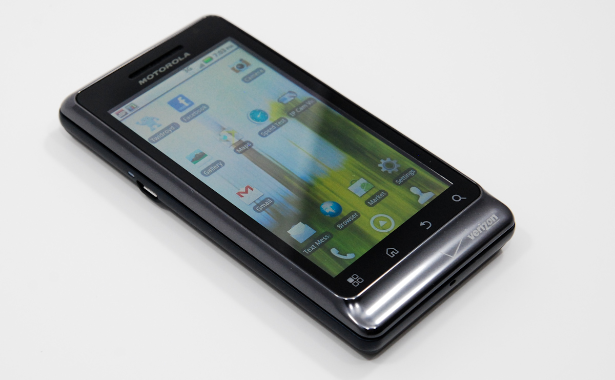
If you’ve played around with the original Motorola Droid, the Droid 2 will feel very familiar. In fact, at first glance, the Droid 2 appears almost identical to its predecessor—so much so that distinguishing the Droid 2 from the original in the hands of passers-by can be a bit of a challenge.

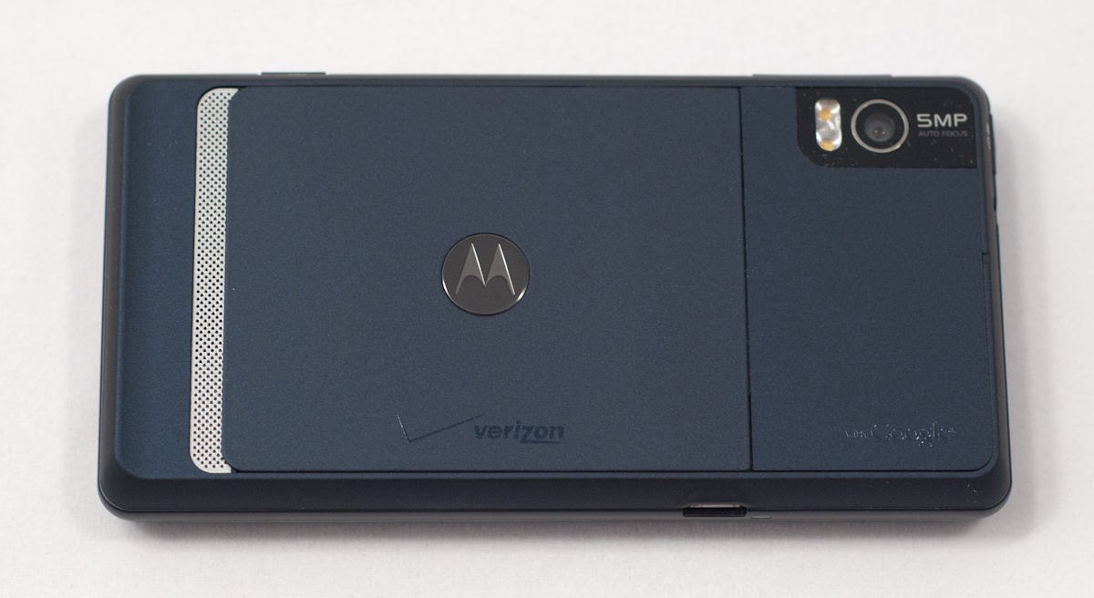
First off, the back of the device isn’t black anymore, it’s a deep navy blue. In fact, basically all of the plastic on the back is a deep navy blue soft touch material. I’m generally not a fan of soft touch backs, as they tend to rub off or discolor from hand grease after a few weeks, but the Droid 2 has done a pretty good job keeping its tack.

The other particularly striking aesthetic change is a dark chrome band running around the top edge of the display. It’s a deeper, darker kind of chrome than I’ve seen on a smartphone before, and gives the Droid 2 a classier look instead of the gaudy fingerprint magnet that chrome usually turns into.

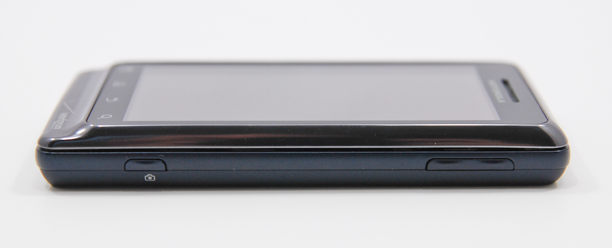
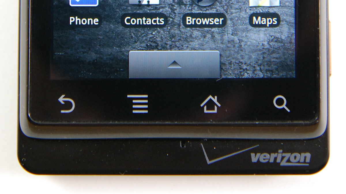
The lip at the bottom is likewise gone, replaced with a tapering chrome slope. Honestly, this space is now somewhat wasted on the Verizon logo. The microphone that used to be here is displaced to the bottom of the device.

The other physical changes are subtle. The previously troublesome volume rocker has been replaced with a much more solid feeling one with less protrusion, and the hard to click camera shutter button also is gone. Both of these changes are perfectly executed—the shutter button is still two step, but now doesn’t require so much force that you change composition when pressing so hard.

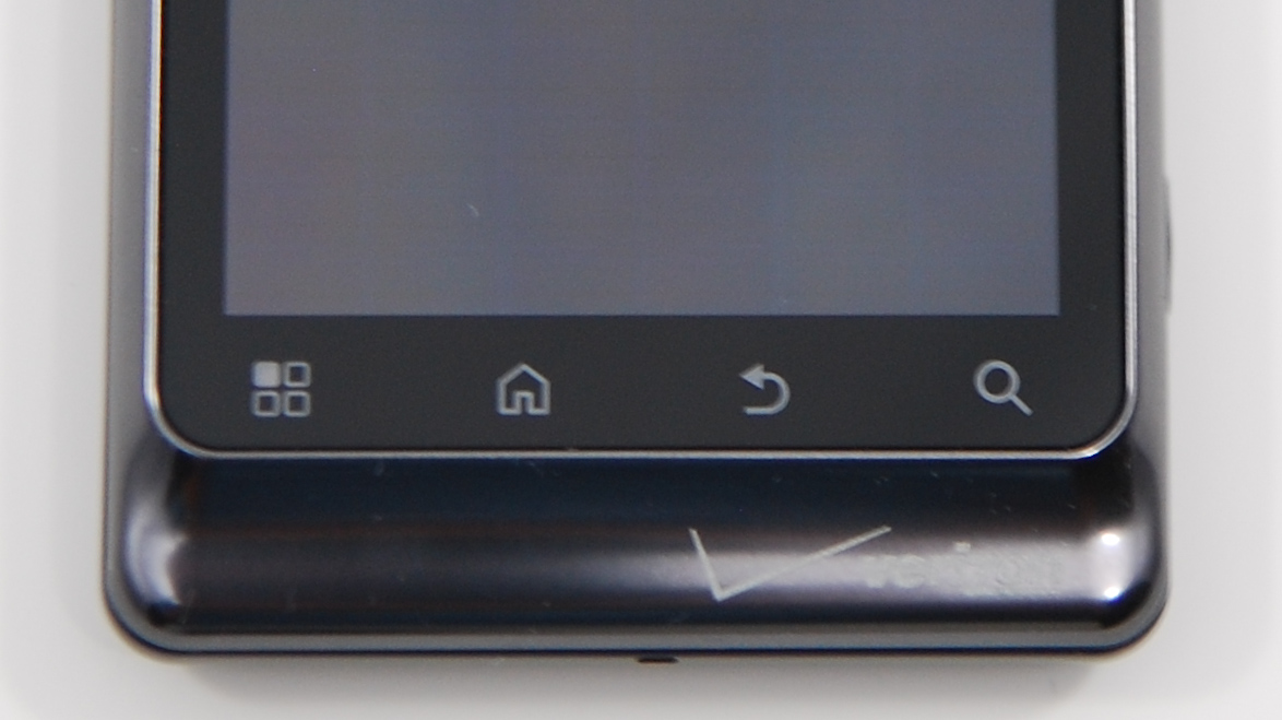
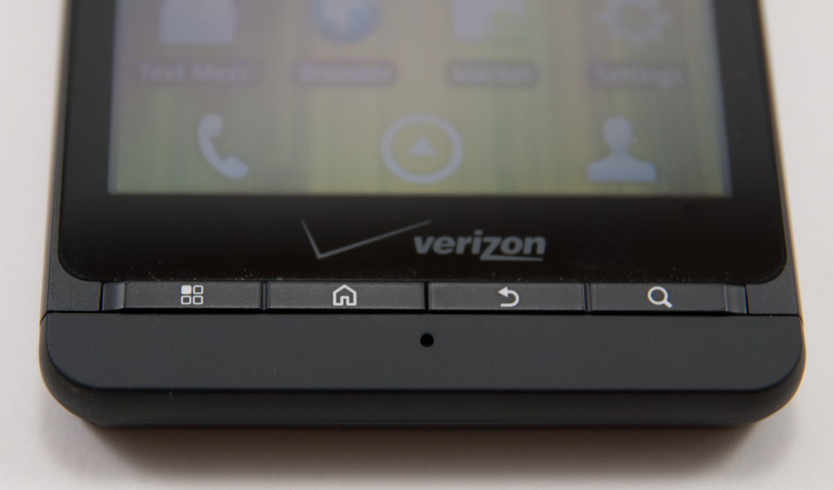
Motorola has kept the same style capacitive buttons from the original Droid, and they work the same as the previous device's. What’s different is the placement.

I’ve already said my piece about this before in the Droid X review. What’s good is that the Droid 2 now has the same button order as said device. What’s bad is that it will no doubt be met with swearing and gnashing of teeth for a few weeks if you’re used to the placement on the original Droid. Hopefully things will settle down now and there will be some standardization. Hey, imagine how I feel regularly using 3 different layouts.

Button Placement—DROID, DROID 2, DROID X

The back of the Droid 2 is essentially the same design, but different colors. The gold speakerphone grating is changed—it’s silver now. As I mentioned, the back is now a navy blue color soft touch material. The camera markings and glass/plastic cover have been moved around a bit, but the camera and flash assemblies themselves appear unchanged.

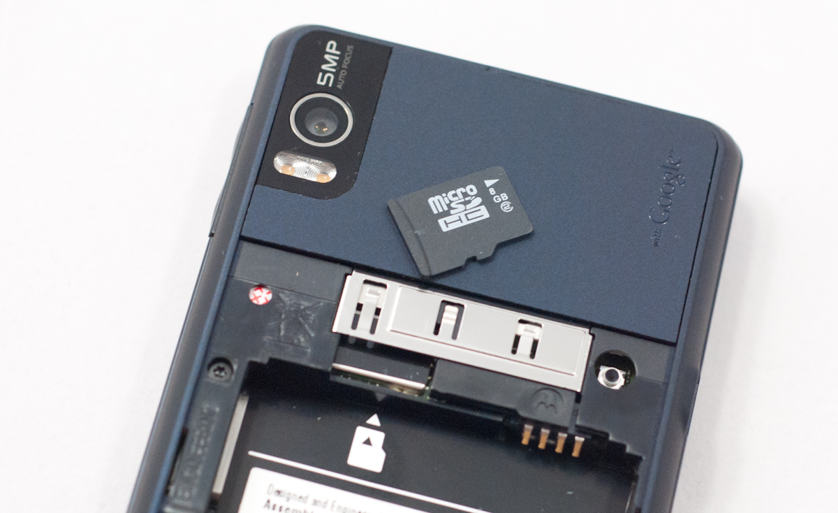
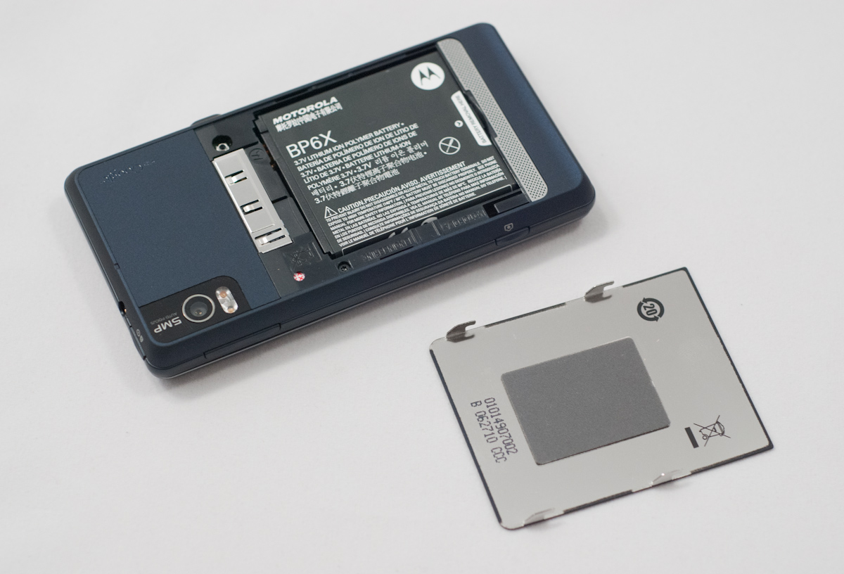
If you pop off the battery door, you’ll discover what lies underneath is basically the same as well. In fact, the Droid 2 appears to use the same BP6X battery the old Droid did, which is a welcome boon for old Droid users—you've now got a backup battery.

The microSD card slot is still not quite optimal, requiring you to slide your thumb along the top and press to get the card out. I strongly prefer press-click-eject designs as I’m constantly worried about breaking or scratching contacts. I guess Motorola doesn’t expect you to be taking the microSD card out a lot. Oh and the card is class 2, not higher performance class 6 like on the Droid X.

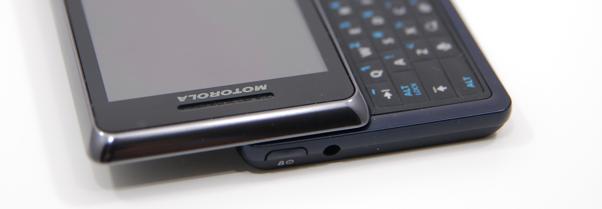
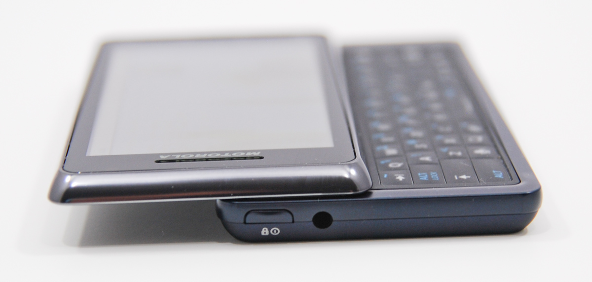
The only remaining subtle tweaks are up top. The power button is similar in shape and style to the other buttons, sporting a rounded top that blends into the case. It’s sometimes a bit hard to locate the power button by sliding your finger along the top of the case, but not impossible.

If you look carefully, there’s also a tiny notch right at the edge between the flat back of the device and the top—this is the port for an internal microphone for noise canceling. I’m a bit concerned this could get blocked with lint or grime. It’s seriously tiny.

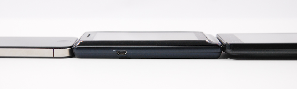
The phone is essentially exactly as slim as its predecessor, but still not super thin. You pay a price in thickness for getting that hardware keyboard (which is excellent—more on it in a second), but not a big one.

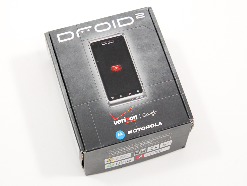
Lastly, the Droid 2’s packaging isn’t anything special or extraordinary. It’s similar to the packaging the Droid X came in, with the device in a nook at the right, and a flip up cardboard piece with accessories underneath. Motorola and Verizon aren’t going for flashy with the packaging, they just want to fit a heck of a lot of them in a box for shipping.


Read more...
Ballmer Names Three New Division Heads at Microsoft


Kurt DelBene has been named president of Microsoft's Office Division, succeeding Stephen Elop, now CEO of Nokia. Microsoft CEO Steve Ballmer also named Andy Lees president of the mobile communications business and Don Mattrick president of the interactive entertainment business. Microsoft faces a battle as Windows Phone 7 debuts.
Microsoft announced Friday three new appointments to head key divisions. In the most prominent appointment, Kurt DelBene has been named president of its Office division, a promotion from his previously position as head of the engineering and development teams in the business division.

The Office division accounts for about a third of the company's annual revenue of about $16 billion. Total revenue for the unit grew 15 percent in the quarter ended June 30, and operating income increased 20 percent.

DelBene, 50, has been with the Redmond, Wash.-based software giant for 18 years, and his team was behind the development of the recently launched Office 2010 products and services. In his new role, DelBene will be responsible for both the engineering and marketing Relevant Products/Services functions for Office, Exchange, SharePoint, Lync, Project, Vision and the company's speech technology Relevant Products/Services.

Andy Lees, Don Mattrick

DelBene replaces Stephen Elop, who recently became the chief executive at Nokia.

At the same time, Microsoft appointed Andy Lees as president of the mobile Relevant Products/Services communications business. A 20-year Microsoft veteran, the 45-year-old Lees was previously senior vice president of the division, and he oversaw the development of Windows Phone 7.

Don Mattrick was named president of the interactive entertainment business. He was senior vice president as the installed base for the Xbox 360 grew to 42 million owners worldwide and more than 25 million Xbox Live users. Mattrick will also be responsible for Kinect, Zune music and video, and PC Relevant Products/Services and mobile interactive entertainment.

"Today's promotions underscore the strength of Microsoft's collective leadership team," CEO Steve Ballmer said, "and set us up well to execute against a powerful lineup of products this fall."

'Major Momentum'

Ballmer added that "not only is the team ready to capitalize on major momentum with our existing products like Office, SharePoint and Halo: Reach, but they are simultaneously bringing entirely new experiences to market with Windows Phone 7 and Kinect for Xbox 360."

Ballmer's references to "major momentum" and "entirely new experiences" reflect the company's effort to overcome some major challenges. On the Office front, Google in particular has compelled Microsoft to adapt its crown jewels into online versions, while many businesses and individuals are looking for reasons why they need to update their existing Office apps.

In mobile, most observers agree that the company dropped the ball with Windows Mobile, losing market share and momentum to Apple's iOS and Google's Android devices in particular. The new Phone 7 is an attempt to get back into that game, a space in which the company must play since the center of gravity for computing has moved to mobile devices.

And in games, the company is hoping its new hands-free controller, Kinect, and increasingly active Xbox Live will give it momentum to continue competing with Nintendo's family-pleasing Wii and Sony's PlayStation.
Read more...